
Within the research there are many teams that they are implemented in the different areas of work. There are even teams that they have been modified to be used in several areas and get more out of it to their functions. This is the case of the electron microscope, it emerged as a upgrade to the optical microscope. And modifications have emerged within it that it even spawned two types. Know the scanning electron microscope and the reasons why it is the favorite of researchers, here.
What is the scanning electron microscope? 🔬👨🔬
Known as SEM for its acronym in English (Scanning Electron Microscope) this is a microscope capable of generating high resolution images. Specifically of the surface of any sample using matter-electron interactions. Its main feature is that it forms the image by using an electron beam instead of a light one.
It was invented by Manfred Von Ardenne in 1937 with the support of in the works that Knoll carried out in the 1930. This equipment sweeps the surface of a sample with an electron beam, obtaining a particle response.
Which receive and analyze the sensors to form the three-dimensional image of the analyzed sample. Currently a scanning electron microscope commercial has a resolution between 04 and 20 nanometers.

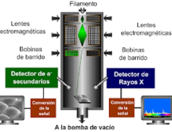
Scanning electron microscope parts 🔬🔌
This microscope has practically the same elements functions of any other electron microscope. Since the differentiation among them, it is realized is by its operating process. Then a below is a list of the main components of a SEM:
- Electron gun: Refers to the source of the electron beam to work.
- Electron lenses: They are responsible for direct and form the beam of the appropriate size.
- Sample area: This is where the holders are placed samples with the material to be analyzed, basically it is the work platform.
- Signal detectors or sensors: They are the responsible for receiving the molecules or particles resulting from the excitation of the sample with the electron beam. Each work area adapts the sensors that they consider relevant according to the work they do.
- Data output devices: They are the screens and other equipment that allow the formation and visualization of the image collected.
Principle of scanning electron microscopy (SEM) 🦠🧫
This principle is a fairly technical process but we will try to describe it in a simple way for your easy understanding. For this reason we will mention it in stages. If you are new to the topic, it is recommended the search for more specific information for better understanding.
We start with the incident beam which are accelerated electrons that carry large amounts of kinetic energy. Which, by impinging directly on the surface of the sample under analysis, dissipates. Generating by means of the sample-electron interaction a significant variety of signals that are recorded by the different sensors.
The different signals emitted in response can be:
Secondary Electrons: They are electrons displacement of the sample components according to the incidence of the beam. Are the ones that generate images in the SEM, especially of topography and morphology.
Scattered retro electrons or BSE: They are employees together with the secondary ones for the creation of the image. Especially from the composition of the sample.
Diffracted back scattered electrons or EBSD: They are used for the determination of crystal structures and location of
mineral.
Photons: X-rays used in the analysis of elements since according to the composition layers lengths are produced specific waves.
Visible Lightheat:
For this reason scanning electron microscopes they always have at least one sensor or detector (secondary electrons). But most have additional detectors that determine their capabilities specify. Its adaptation depends on the operation that will be given in the area let it be employed.
Then once the sensors receive the signals specific, it gives way to the formation of the image that will be exhibited in the screen. The interesting thing about this analysis is that it can be performed on multiple opportunities since it does not cause damage, nor decrease in volume in the study.
Applications of SEM 🔬🧬
Generate high-resolution images of the shape of the objects.Provide maps of the elemental composition or chemical analysis of specific areas.Discriminating phases using BSE.Accurately measure items and objects up to 50 nano meters.Examine microfiber orientation and crystallographic in materials.
Advantages and disadvantages of scanning electron microscope 👩🔬🖤
Advantage
- It can be said that there is no other team with the amount of applications that the SEM has in the study of solid materials.
- They are easy to operate if the personnel in charge fully know its operation.
- It requires minimal sample preparation in most of its applications.
- It they acquire data quickly in most of their modalities, approximately in five minutes.
- They generate data in digital format that can be reported and even be shared.
Disadvantage
- Only solid samples that enter the camera intended for the sample in the microscope.
- The maximum sizes are a little reduced by having 10 centimeters for the horizontal dimension.
- While which for the vertical dimension is just 40 millimeters.
- Samples should be stable in the presence of vacuum.
- EDS sensors do not detect very light elements and they also have problems with low atomic numbers.
- It has many requirements of infrastructure for its use.
- Such as a system of cooling, power supply, vacuum system, vibration-free floor, isolated room free of magnetic fields.
Ready you already know the scanning electron microscope completely and it is no surprise that it is the favorite. Due to its large number of applications and the specificity of its results, it is the best tool for the study of solid matter. If you want to know a little more about laboratory materials, take a look at the rest of our publications.